 Precision Machinery Technology Co., Ltd")


For large test components such as silicon wafers and sapphire wafers, the AOI1000 Optical Component Surface Defect Detector offers a detection resolution of up to 0.5 micrometers and a maximum inspection aperture of 1000mm by 600mm. The device is capable of automatically generating reports, with report formats including the U.S. Military Standard MIL-PRF-13830A/B and the International Standard ISO 10110-7.
|
product name |
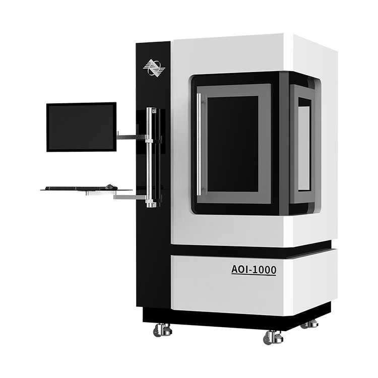
AOI1000 Optical Component Surface Defect Detector |
|
Maximum detection size |
1000mmX600mm |
|
Detection resolution |
0.5μm |
|
Detection method |
Dark field array scanning imaging |
|
Output reports |
National standards, U.S. military standards, and customized enterprise reports. |
The AOI1000 Optical Component Surface Defect Detector uses machine vision technology to achieve automated, high-speed, and high-precision detection of surface defects on components such as silicon wafers and sapphire wafers, effectively addressing the issues of low efficiency and poor accuracy in visual inspection. The highest detection resolution can reach 0.5 micrometers, and the maximum detection aperture can be as large as 1000mm by 600mm. The imaging technology includes annular illumination and micro-scatter dark field imaging. The device is capable of automatically generating reports in various formats, including the U.S. Military Standard MIL-PRF-13830A/B and the International Standard ISO 10110-7.

Suitable for quality control of surface defects in optical components, optical window wafers, silicon wafers, sapphire wafers, etc.
Coating defects: delamination, damage to the coating, etc.
Polishing defects: scratches, pits, chipping, bubbles, dirt, etc.
This equipment can handle the following types of defects:
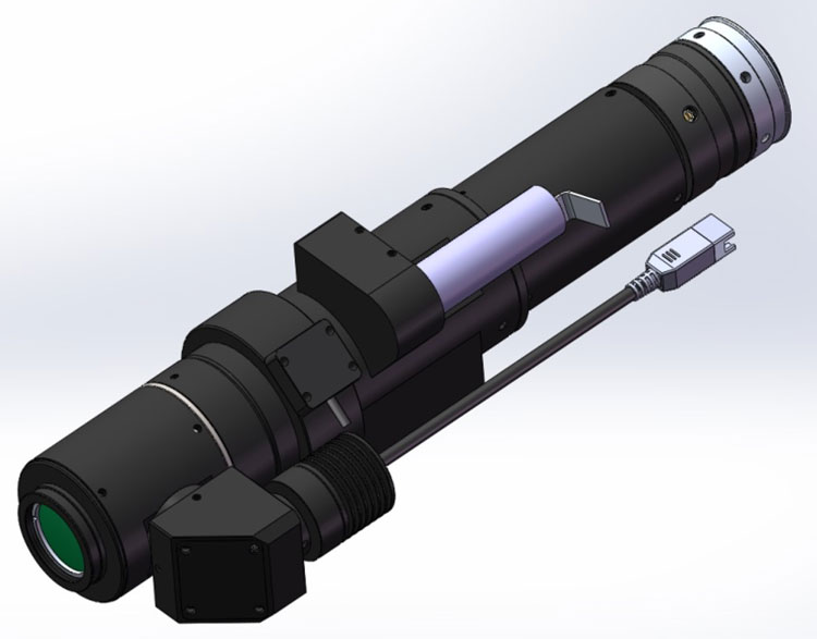
◆ Multi-beam annular illumination
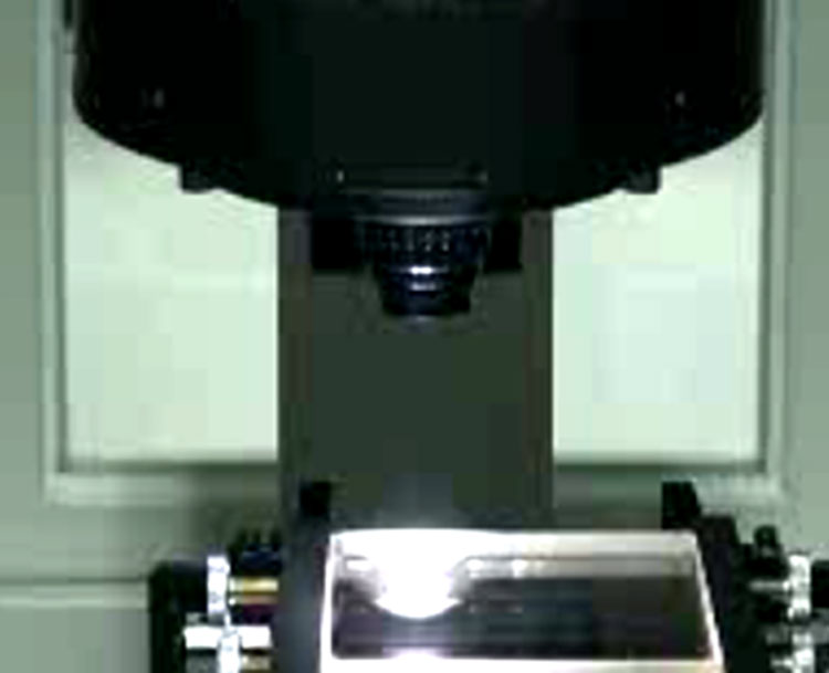
◆ Variable magnification imaging with high and low magnification options
◆ Detection accuracy of 0.5 μm
◆ Whole-plate multi-wafer detection
◆ Linear motor for rapid imaging
◆ Equipped with an FFU (Fan Filter Unit) to ensure internal cleanliness
Multi-beam annular imaging illumination
Automatic zoom microscope from 1X to 8X.
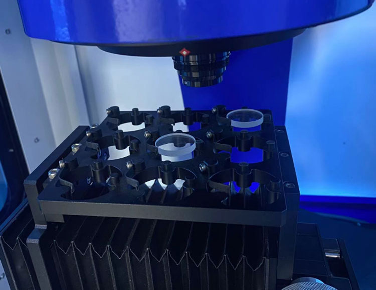
Adjustable rapid clamping for the entire plate.
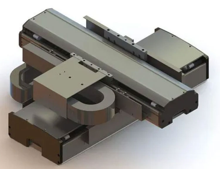
High-precision 2D linear motors ensure the accuracy of rapid shooting.
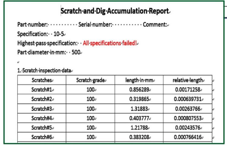
Military standard spreadsheet output
Test result display

Coating surface scratch.
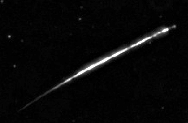
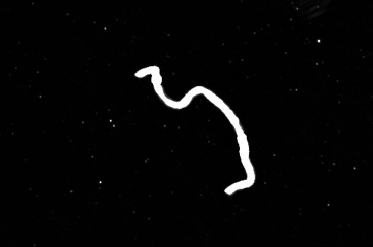
Scratches

Laser damage spot 1

Laser damage spot 2

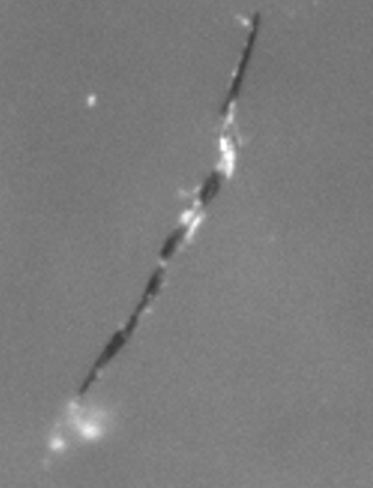
Nanoscale particulate point
Fiber

Component deliquescence
membrane layer damage
|
AOI450 Optical Component Surface Defect DetectorAOI1000 Optical Component Surface Defect Detector |
|
|
Item |
Description |
|
Model |
AOI1000 |
|
Equipment Function |
Quantitative defect detection for ultra-smooth surface planar optical components, and output of electronic reports according to the detection results such as U.S. Military Standard, National Standard, and International Standard. |
|
Maximum Detection Size |
1000mmX600mm |
|
Detection Precision |
Low magnification 5μm, high magnification 0.5μm |
|
Clamping Method |
Whole plate clamping or single piece clamping, supporting square and round piece clamping. |
|
Leveling Method |
Whole plate material assisted automatic focusing, electric leveling. |
|
Imaging Method |
Annular illumination, micro-scatter dark field imaging, in accordance with the "Quantitative Detection Method for Surface Defects of Optical Components—Micro-scatter Dark Field Imaging Method" described in the national standard GB/T 41805-2022. |
|
Detection Method |
Low magnification scanning stitching, high magnification positioning quantification. |
|
Scanning Mechanism |
2D linear motor, stroke 150mm × 150mm. |
|
Camera Parameters |
Large target camera, 5 million pixels. |
|
Report Format |
Excel, Word format, U.S. Military Standard, National Standard, International Standard, or enterprise statistical report. |
|
Industrial PC Config |
i7 processor, 32GB memory, 1T hard disk, 6GB video memory. |
|
Equipment Dimensions |
900mm × 800mm × 2000mm (L × W × H) |
|
Power Supply Voltage |
220V ± 10% |
Address
No. 578 Yingkou Road, Yangpu District, Shanghai, China
Tel


")


")